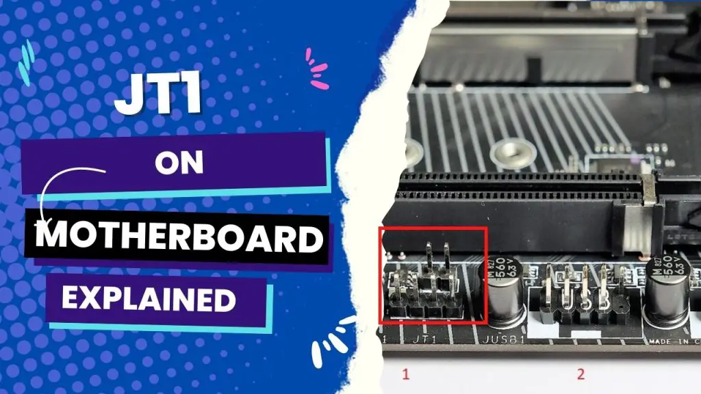
JT1 is a debug port on a motherboard that tests the CPU’s power supply. It can be used with special tools like a debug card or multimeter to find and fix problems with the motherboard or other hardware. Technicians can talk to and watch the behavior of motherboard devices in real-time through the port. To use JT1, you may need a compatible cable and specialized software or instructions.
If you just got a motherboard, you may notice that it has several connectors not covered by the manual, such as the JT1, JDP1, JBD1, and JSMB1 (this is near the JCI1 chassis intrusion).
This article will focus on the JT1 ports, and I guess you are wondering what they do and, more importantly, what goes into them. Well, if you initially assumed that some of these ports were debugged or service ports, your assumptions are quite right. But there’s more.
In this article, I have laid out comprehensive information on the JT1 on motherboards, its function, how to use it, and what the pin layout of the JT1 connector looks like on different motherboards.
What is the JT1 connector for?
JT1 is also called the Joint Test Action Group (JTAG) connector, but this is not a common industry name. The port is a hardware interface that primarily functions for the manufacturing and testing of motherboards, as well as in system maintenance and troubleshooting. What does this mean?
On a motherboard, the JT1 connector will access the JTAG interface of various devices, e.g., the CPU, memory, and other integrated circuits, allowing technicians to perform various tests and troubleshooting tasks.
In other words, the connector aids in the verification of device functionality and problem diagnosis. Sometimes, the JT1 connector aids in firmware updates or programming of the devices.
The JTAG comprises a set of protocols and electrical signals that allow a device to access and control the internal components of a device connected to the JTAG interface to test and debug circuits on printed circuit boards (PCBs).
Pin Layout of the JT1 Connector on Motherboards
There is no standard physical description of the JT1 connector on motherboards, as it varies depending on the specific board model and devices that support it. However, the connector is generally a small, rectangular header near the PCB’s edge on most motherboards.
Some models have a plastic cover that serves as a shield for the pins. But some models do not have this feature.
The typical JT1 connector features between 4 and 20 pins. The number of pins on the connector depends on the number of devices that the JTAG interface needs to be connected to.
JT1 would include some signals, depending on specific motherboards. These signals include the TCK, RTCK, TDI, and others. (More on this in the next section.)
JT1 Signals on Motherboards and Their Meaning
The number of signals on the JT1 connector depends on the connection requirements of the JTAG interface. It will typically feature the following:
| JT1 Signal | Meaning |
| TMS | It means Test Mode Select and is used to choose the mode of operation, such as debug or test mode. |
| RTCK | It means “Return Test Clock” and is used to confirm the validity of the data received by the device being tested. |
| TDO | It means “Test Data Out” and displays the data from the tested device. |
| TCK | The test clock signal synchronizes the data transfer between the tester and the tested device. |
General Uses of JT1 Connectors on Motherboards
The generic response to what JT1 is used for in motherboards is a system maintenance and troubleshooting. But technically, the connector is used for diagnosing and fixing issues with the devices on a motherboard.
In addition, the JT1 connector updates the firmware or programming of the devices connected to the JTAG interface whenever there is a bug in the firmware. It also helps with the update when a newer version of the firmware offers extra fixes or features.
I advise you to seek the assistance of a qualified technician if you are not comfortable using the JT1 connector for system maintenance and troubleshooting. Improper use of the connector can damage the connected device or the motherboard itself.
Closing Remark
The first time I had an issue dealing with JT1 was when I first got an X470 Pro Carbon motherboard and noticed a four-pin connector that was not mentioned in the manual. The silver lining is that your motherboard will probably identify the connector as JT1, which is easily located around the JCI1—next to the JUSB1.
If you have been wondering what JT1 is and what it is used for, the answer isn’t as complicated as it may seem. First, you need to understand that
The JT1 connector is an important part of the design and maintenance of motherboards, as it allows technicians to communicate with and debug the devices connected to the JTAG interface. If you aren’t used to fixing motherboards, you may want to leave this part for the experts.
But with what we’ve touched on in this post, I believe you can make decisive steps toward using the connector, especially for updating the firmware or programming of the devices connected to the JTAG interface to fix bug issues.
Meanwhile, there are debugging technologies, such as serial and parallel ports. Still, in my opinion, the JT1 connector offers some advantages, such as its high-speed data transfer capabilities, access to a wide range of devices on a motherboard, and ability to operate in a low-power state, make it more well-suited.


![How to Add More SATA Ports to Motherboard? [Guide] 5 How to Add More SATA Ports to Motherboard](https://bestofmotherboard.com/wp-content/uploads/2022/02/How-to-Add-More-SATA-Ports-to-Motherboard.jpg)
![How To Install Motherboard Drivers With USB? [Guide] 6 How To Install Motherboard Drivers With USB](https://bestofmotherboard.com/wp-content/uploads/2022/02/How-To-Install-Motherboard-Drivers-With-USB.jpg)